Top 5 Benefits of Using Multilayer PCB in Electronic Devices
In the rapidly evolving world of electronics, the demand for compact, efficient, and high-performance devices is ever-increasing. Among the various innovations that have emerged to meet these needs,
multilayer PCB technology stands at the forefront. By integrating multiple layers of circuitry into a single board, multilayer PCBs offer decisive advantages over traditional single or double-layer boards, enabling manufacturers to create more sophisticated electronic devices with improved functionality and reliability.
The benefits of using multilayer PCBs in electronic devices extend beyond mere space-saving. These advanced circuit boards enhance electrical performance by minimizing signal loss and electromagnetic interference, which is crucial for the seamless operation of modern gadgets. Furthermore, multilayer PCBs facilitate more intricate designs, allowing for complex routing of power and signals that support advanced features in devices ranging from smartphones to medical equipment.
As we delve into the top five benefits of multilayer PCBs, it becomes clear that their adoption is not merely a trend but a necessity for those seeking to stay competitive in the fast-paced electronics industry of 2025 and beyond.
Advantages of Multilayer PCBs: Enhancing Compactness in Electronic Design
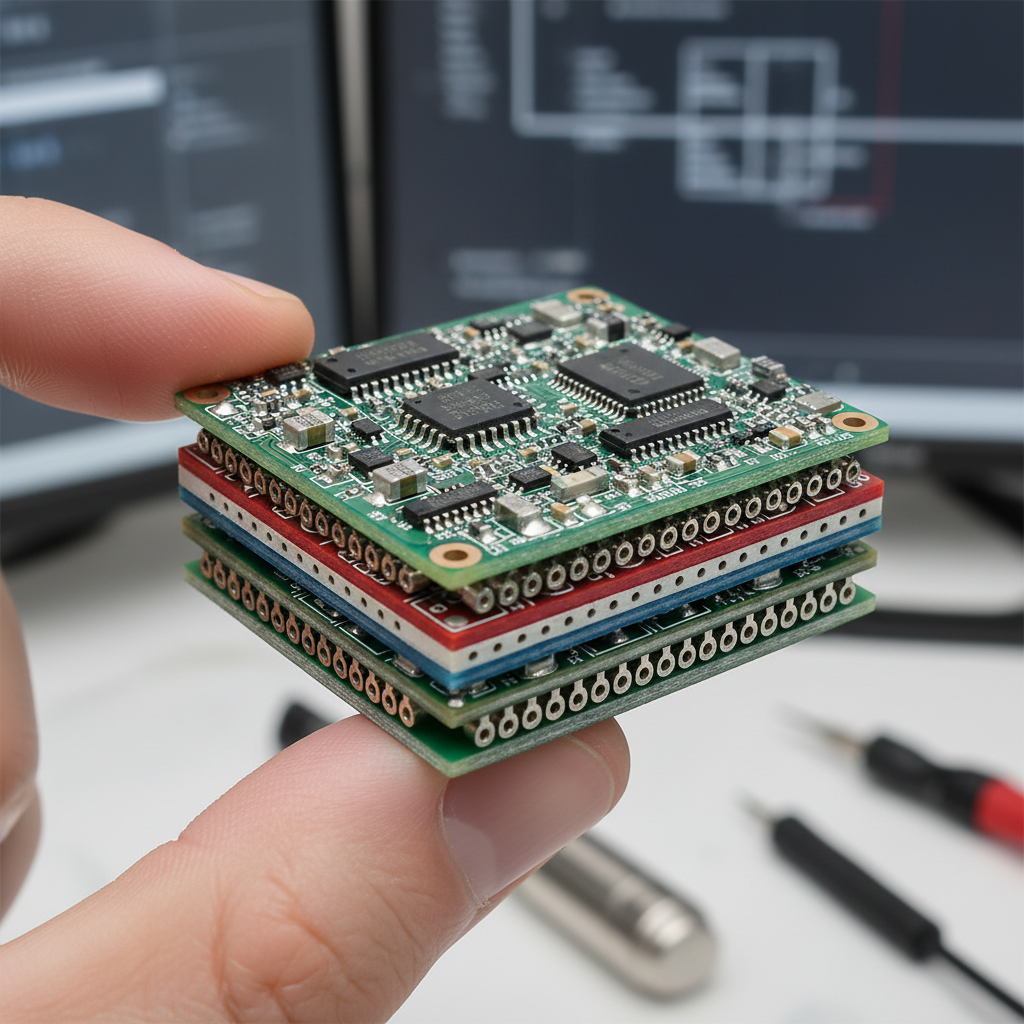
Multilayer PCBs (Printed Circuit Boards) are revolutionizing the landscape of electronic design by significantly enhancing compactness without compromising functionality. As electronic devices become increasingly miniaturized, the need for efficient space utilization becomes critical. A multilayer PCB accommodates more circuitry within a smaller footprint, allowing designers to place numerous components in a compact arrangement. This is particularly beneficial in handheld devices where space constraints can limit performance and capabilities.
In addition, multilayer PCBs improve signal integrity and reduce electromagnetic interference (EMI), which is crucial in high-speed applications. By layering multiple circuits, designers can strategically route signals and ground planes, leading to improved performance and reliability. This compact design not only streamlines the manufacturing process but also opens up new possibilities for innovative product designs, ultimately enhancing user experiences in today’s technology-driven world. As a result, multilayer PCBs are becoming an essential component in the pursuit of more advanced and efficient electronic devices.
Cost Efficiency: Long-Term Savings from Reduced Board Count in Production
The rising demand for efficient and compact electronic devices has led to an increased adoption of multilayer PCB designs. One significant benefit of using multilayer PCBs is cost efficiency, particularly through long-term savings achieved by reducing the number of boards required in production. By integrating multiple layers into a single PCB, manufacturers can streamline their processes, cut down on material expenses, and minimize labor costs associated with assembly.
According to recent industry reports, the offline PCB laser depaneling systems market is projected to grow from $141.41 million in 2024 to $203.26 million by 2032, reflecting a CAGR of 4.7%. This growth indicates an expanding recognition of advanced manufacturing techniques that leverage multilayer designs to enhance production capabilities. As artificial intelligence and automotive sectors continue to evolve, the demand for higher computational power emphasizes the need for efficient PCB solutions capable of meeting stringent performance standards while optimizing costs.
Consequently, the implementation of multilayer PCBs not only supports the miniaturization and densification of electronic systems but also ensures manufacturers can maintain competitive pricing while navigating the complexities of modern electronic design and production. By taking advantage of these technologies, businesses are well-positioned to capitalize on emerging market trends and technological advancements.
Improved Signal Integrity: Minimizing Crosstalk in High-Frequency Applications
In the realm of high-frequency applications, signal integrity is paramount, and multilayer PCBs play a critical role in achieving optimal performance. By offering multiple layers for routing signals and power, multilayer PCBs significantly reduce crosstalk, which is the unwanted transfer of signals between circuit traces. According to a 2022 report by IPC, over 75% of electronic design engineers identified crosstalk as a leading cause of signal integrity issues in high-speed circuits. By implementing a well-designed multilayer PCB, designers can enhance the separation between signal layers, effectively minimizing noise and ensuring cleaner signals.
Additionally, multilayer PCBs allow for optimized impedance control, which is essential for high-frequency applications. With tighter control over impedance discontinuities, these PCBs greatly enhance the quality of signal transmission. A study published in the IEEE Transactions on Microwave Theory and Techniques revealed that PCBs with four or more layers can reduce signal degradation by up to 50% compared to traditional two-layer designs. This improvement is crucial for applications such as RF communications, where signal clarity directly impacts overall system performance. Overall, multilayer PCB technology equips engineers with the ability to design robust, high-performance electronic devices that can handle today’s demanding frequencies with ease.
Thermal Management: Effective Heat Dissipation Strategies in Multilayer Designs
Multilayer PCBs (Printed Circuit Boards) provide significant advantages in thermal management, particularly for high-performance electronic devices. Effective heat dissipation strategies are crucial as components become increasingly compact and power-dense. Multilayer designs allow for optimized heat pathways, enhancing both in-plane and through-plane thermal conductivity. By integrating specialized materials and strategic layer arrangements, multilayer PCBs can dissipate heat efficiently, minimizing the risk of overheating and prolonging the lifespan of electronic components.
Tips for maximizing thermal management in multilayer PCBs include conducting thermal simulations during the design phase to predict heat flow and effectiveness, selecting materials with high thermal conductivity, and considering additional cooling methods such as heat sinks or thermal interface materials. When designing for thermal performance, keeping component placement in mind can also help facilitate better airflow and heat distribution.
Moreover, the incorporation of multilayer strategies not only aids in thermal management but also contributes to overall system performance. Using multi-filler composites can enhance thermal conductivity, creating a synergistic effect that further boosts heat dissipation capabilities. This careful material design, combined with multilayer techniques, is essential for the reliability and efficiency of modern electronic devices.
Top 5 Benefits of Using Multilayer PCB in Electronic Devices - Thermal Management: Effective Heat Dissipation Strategies in Multilayer Designs
| Benefit |
Description |
Heat Dissipation Strategy |
Application |
| Improved Thermal Management |
Multilayer PCBs can efficiently manage and dissipate heat, preventing overheating. |
Copper planes act as thermal sinks. |
High-performance computing. |
| Reduced Size and Weight |
Allows for a compact design, which is essential in portable devices. |
Use of buried and blind vias. |
Smartphones and tablets. |
| Enhanced Signal Integrity |
Improved grounding and shielding reduces interference. |
Ground planes provide effective shielding. |
Communication devices. |
| Cost-Effective Manufacturing |
Reduction in assembly time and materials can lower costs. |
Fewer layers can streamline the production process. |
Consumer electronics. |
| Increased Reliability |
Robust design reduces chances of failure due to heat-related issues. |
Thermal vias improve heat path. |
Automotive applications. |
Scalability and Flexibility: Adapting Multilayer PCBs for Future Tech Requirements
In the fast-evolving landscape of technology, the scalability and flexibility of multilayer printed circuit boards (PCBs) have become crucial in addressing future tech requirements. As electronic devices become more complex, the need for efficient space utilization and enhanced functionality increases. Reports by market research firms like Allied Market Research indicate that the global multilayer PCB market is projected to reach USD 37.32 billion by 2027, reflecting a compound annual growth rate (CAGR) of 4.3%. This growth is driven by the rising demand for advanced electronic devices, including smartphones and IoT devices, which require high-density interconnects that multilayer designs uniquely provide.
Moreover, multilayer PCBs allow for easier adaptation to new technologies, offering the flexibility to incorporate emerging components without requiring extensive redesign. This adaptability is essential as companies seek to innovate rapidly to stay competitive. The capacity to incorporate multiple layers facilitates complex circuitry, enabling device manufacturers to optimize size and performance. According to a study by ResearchAndMarkets, multilayer PCB technology can significantly reduce the time from concept to market, allowing companies to respond swiftly to consumer demands and technological shifts, showcasing how this versatility supports sustained industry growth and innovation.