10 Essential Tips for Designing a Successful PCB Board

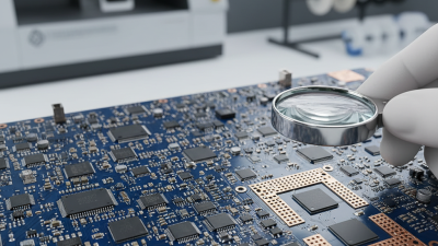
Designing a successful PCB board can be both exciting and challenging. Whether you are a seasoned engineer or a beginner, these tips will guide you. A printed circuit board (PCB) is crucial for electronic devices. It connects various components efficiently.

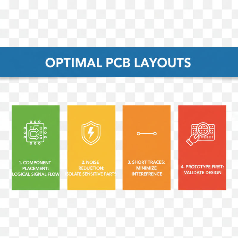
Attention to detail matters. Each component placement affects the board's functionality. Consider your design's requirements carefully. Don't overlook the importance of track width and spacing. These factors influence current behavior and signal integrity. Mistakes in these areas can lead to malfunction. Reflect on your design choices often.

Embrace feedback from peers. Collaboration can enhance your design process. View each review as a learning opportunity. Experiment with different layouts. Try to optimize your design, even if it’s already good. Each iteration can lead to significant improvements. Designing a PCB board is more than just technical skills; it’s about creativity and adaptability.

10 Essential Tips for Designing a Successful PCB Board

Understanding the Basics of PCB Design and Its Importance

Designing a printed circuit board (PCB) is crucial in electronics. A well-executed design enhances performance and reliability. Mishaps in PCB design can lead to significant failures. In fact, nearly 30% of all electronic product defects arise from PCB issues, according to a 2022 report by IPC, the global trade association. This emphasizes the importance of understanding essential design principles.


Knowing the basics of PCB design helps prevent costly errors. The layout, component placement, and routing must all be carefully considered. Poor routing can increase electromagnetic interference, affecting signal integrity. It's essential to balance functionality and manufacturability. However, many designers overlook this aspect, leading to production problems later on.


Another common mistake is not accounting for thermal management. Heat sinks and adequate spacing can minimize thermal buildup. Reports indicate that improper heat management accounts for around 10% of PCB failures. Design tools can aid in creating an optimized layout. Yet, these tools cannot replace the need for a solid foundational understanding of PCB design principles. It’s a complex balance that often requires revisions and adjustments.

Selecting the Right Materials for PCB Fabrication

10 Essential Tips for Designing a Successful PCB Board

When designing a PCB board, material selection plays a vital role. The choice of materials affects both performance and manufacturing processes. Different materials have distinct properties. For example, FR-4 is common for its balance of cost and performance. However, it may not be ideal for high-frequency applications.

Consider thermal management as well. Materials like aluminum or copper can provide better heat dissipation. They are often overlooked but essential. If the wrong materials are used, the board can fail under stress. This can lead to costly redesigns and delays.

Also, think about the environment. Some materials may not withstand humidity or extreme temperatures. This can impact the board's longevity. A lack of foresight in material choice can result in unexpected challenges. Addressing these concerns early helps in creating a robust design. Ultimately, the right materials ensure reliability and efficiency in your PCB.

Designing Effective PCB Layouts for Optimal Performance

10 Essential Tips for Designing a Successful PCB Board

Designing effective PCB layouts is crucial for achieving optimal performance. Start by considering your component placement. It should ensure a logical flow of signals. Place sensitive components away from high-frequency noise sources. Keep traces short to minimize interference. It often helps to prototype layouts before finalizing the design.

Next, think about grounding and power distribution. Layout a solid ground plane to reduce electromagnetic interference. Ensure adequate power supply to all components. Uneven power distribution can cause malfunctions. It's worth reflecting on the common pitfalls in this area. Be wary of trace widths; inadequate widths can lead to overheating.

Consider thermal management as well. Components generate heat, which can affect performance. Use thermal vias and heat sinks where necessary. Testing the heat dissipation early is vital. Mistakes in this area often lead to reliability issues. A good layout should not just work, but also work well over time.

Best Practices for Testing and Debugging PCB Boards

Testing and debugging PCB boards is a critical aspect of the design process. Data shows that nearly 30% of all PCB failures arise from design errors. Such errors often occur during the testing phase, signaling the need for robust debugging techniques. Utilizing advanced testing methods like Automated Optical Inspection (AOI) or X-ray inspection can detect issues early, reducing the risk of costly revisions later in production.

In practice, engineers must always remain vigilant. Even minor flaws can lead to significant failures. A recent survey revealed that nearly 40% of engineers reported difficulties in identifying hidden faults in complex PCB boards. To address this, maintaining a structured testing approach is vital. Conducting multi-stage testing, including functional and performance testing, helps streamline the identification of issues. Also, peer reviews during the debugging phase often reveal overlooked errors, leading to improved outcomes.

While no method guarantees a flawless PCB design, a disciplined approach is essential. Relying solely on automated tests may miss certain nuances. Balancing technology with manual inspection can bridge this gap. Always consider documenting the debugging process. This not only aids in current projects but also serves as a reference for future designs, honing your skills over time.

10 Essential Tips for Designing a Successful PCB Board

This bar chart illustrates the importance of different design practices in PCB design and their corresponding success rates based on industry surveys.

Common Mistakes to Avoid in PCB Design Processes

In the world of PCB design, avoiding common mistakes is crucial for success. A report by IPC states that 30% of PCB failures stem from design errors. These can include incorrect component placements or inadequate trace widths. Attention to detail is paramount.

Many designers overlook thermal management. Proper heat dissipation is critical to prevent component damage. Ensure that your design accommodates sufficient airflow and heat sinks. Remember, a well-designed thermal layout can be the difference between a functional board and a failure.

Another common pitfall is neglecting signal integrity. High-frequency signals need careful routing. Avoid long trace lengths and sharp angles. The goal is to minimize interference and ensure reliable performance. Regularly reviewing your design against best practices can help catch these issues early.

Aiming for perfection is admirable, but embracing flaws can lead to growth. Learning from design missteps helps refine skills. Each mistake brings valuable insights that can enhance future projects.

10 Essential Tips for Designing a Successful PCB Board - Common Mistakes to Avoid in PCB Design Processes

Tip Description Common Mistake
1. Understand the Basics Familiarize yourself with PCB design fundamentals including materials and manufacturing methods. Skipping foundational knowledge can lead to improper designs.
2. Choose the Right Components Select components that fit your design requirements and are readily available. Using outdated or hard-to-source components can delay prototypes.
3. Optimize Layout Efficiently arrange components to minimize trace lengths and improve signal integrity. Poor layout can lead to performance issues.
4. Consider Power Requirements Design for adequate power distribution and thermal management. Neglecting power needs can result in component failure.
5. Utilize Simulation Tools Leverage software to simulate circuit behavior before production. Ignoring simulations can lead to overlooked design flaws.
6. Design for Testability Incorporate test pads and access points into the design. Not planning for tests can complicate debugging.
7. Follow Design Guidelines Adhere to best practices and industry standards for PCB design. Ignoring standards might lead to compliance issues.
8. Plan for the Future Design layouts that can accommodate future upgrades. Static designs limit future enhancements.
9. Perform Full DRC Checks Conduct Design Rule Checks to ensure all specifications are met. Skipping DRCs can lead to costly manufacturing errors.
10. Review and Revise Have your design reviewed by peers for feedback and improvements. Failing to seek feedback can perpetuate design flaws.

Search our website