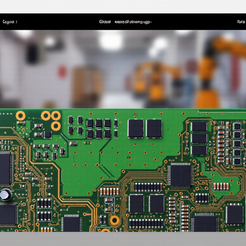
A pcb circuit board is the quiet framework behind most modern electronic devices. It connects components, guides electrical signals, and supports reliable operation inside phones, vehicles, computers, and industrial controls. Without it, a circuit becomes a loose collection of parts, wires, and uncertain connections.
Paul Eisler, widely recognized as the inventor of the printed circuit board, said, “The printed circuit is the basic building block of modern electronics.” His observation remains relevant today. A board uses copper traces, insulating layers, solder masks, and drilled holes to create controlled electrical pathways. Components attach to these pathways through soldered joints. Small details matter. A weak joint can create heat, noise, or complete failure.
This article explains what a pcb circuit board is and how it works. It will examine its layers, materials, manufacturing stages, and role in signal transmission. It will also clarify the difference between a bare board and an assembled circuit board. That distinction is often overlooked.
Real engineering is less perfect.
Designers must balance cost, size, heat, durability, and performance. A compact board may save space but complicate repair. Thicker copper can improve current handling but increase production costs. Even a carefully designed board can fail when moisture, vibration, or poor assembly enters the picture. Understanding these limits helps readers evaluate technical claims more responsibly. The following sections connect basic theory with practical examples, including visible copper tracks, component placement, and the testing methods used before a board reaches a finished product.
What Is a PCB Circuit Board?
A PCB, or printed circuit board, is a rigid or flexible platform that connects electronic components. It uses conductive copper paths instead of loose wires. These paths carry electrical signals and power between parts. The board also provides mechanical support, so components stay aligned during operation.
A typical PCB contains several layers. Fiberglass or another insulating material forms the core. Thin copper layers are etched into precise patterns. A protective coating covers most exposed copper, while small pads remain available for soldering. Components may include resistors, capacitors, connectors, sensors, and integrated circuits. Tiny drilled holes can connect copper paths between different layers. This structure saves space and makes circuit assembly more consistent.
When power enters the board, copper traces guide current toward the required components. A resistor can limit current, while a capacitor can store and release electrical energy. Integrated circuits process signals according to their internal design. I have seen a board appear simple while hiding complex routing beneath its surface. That is where a basic definition becomes incomplete. Trace width, heat, signal interference, and manufacturing tolerances can affect reliability. Engineers must check these details with electrical calculations and design software. Even then, a first design may need revision after testing. A silkscreen label can help inspection, but it cannot correct a poor circuit layout.
What Is a PCB Circuit Board and How Does It Work?
A PCB is a layered platform that connects electronic components through controlled electrical paths. Its main base is the substrate, usually a rigid or flexible insulating material. Copper layers form the conductive routes, called traces. These traces carry signals and power between parts. The board may have one, two, or several copper layers.
The most visible parts include pads, vias, solder mask, and silkscreen markings. Pads are exposed copper areas where components are soldered. Vias are tiny plated holes that connect traces between layers. The solder mask covers most copper and helps prevent accidental contact. Silkscreen labels identify component positions and polarity. Resistors, capacitors, connectors, and integrated circuits sit on these prepared areas. During inspection, a technician may notice a darkened pad, a lifted trace, or uneven solder around a pin. Small details matter.
Tips: Check the board under bright, angled light. Look for cracked solder joints, missing components, and copper exposed outside its intended path. A clean appearance does not prove perfect operation. Electrical testing is still necessary. Also, circuit layouts involve trade-offs. A shorter trace may reduce signal delay, yet it can create tighter spacing and harder repairs. Designers must balance performance, heat, manufacturability, and future maintenance. Mistakes are sometimes subtle.
A PCB circuit board is a rigid platform that connects electronic components through copper paths. Its layers are bonded together with insulating material and carefully aligned. A common four-layer board contains two signal layers and two power or ground planes. The top layer holds components, solder pads, and visible traces. The bottom layer often carries additional routing and smaller components. Copper planes provide stable electrical reference points and help distribute current.
Connections move between layers through plated holes called vias. A via may pass through the entire board or connect only selected layers. Designers place traces according to current, voltage, frequency, and available space. High-current paths usually need wider copper. Sensitive signals need short, controlled routes. Parallel traces can create unwanted interference, especially when they share long distances. Small details matter.
The layer arrangement is called the stackup. It affects signal integrity, heat flow, manufacturing cost, and mechanical strength. During practical inspection, engineers check trace widths, clearance, via quality, and solder joints under magnification. A ground plane can reduce noise, but it does not fix every layout mistake. That assumption is worth challenging. Poor return paths may still cause unstable measurements, even when the schematic appears correct. Thermal vias beneath a hot component can move heat into an inner plane, although their effectiveness depends on copper area and board construction. Real boards often require adjustment after testing.
| PCB Element or Concept | Typical Structure or Data | How It Works | Design Considerations |
|---|---|---|---|
| Printed Circuit Board (PCB) | A rigid or flexible board that mechanically supports electronic components and electrically connects them. | Copper conductors carry power and signals between components without requiring separate point-to-point wires. | The board material, layer count, copper thickness, and layout must match the electrical, mechanical, and thermal requirements. |
| Core or Laminate Material | Insulating material, commonly a glass-fiber-reinforced epoxy laminate, separates conductive copper layers. | The dielectric prevents unintended electrical contact while providing mechanical strength. | Important properties include dielectric constant, dielectric loss, thermal stability, moisture resistance, and thickness. |
| Copper Layer | Thin copper foil or plated copper used for signal traces, power planes, and ground planes. | Copper provides a low-resistance path for electrical current and high-frequency signals. | Common nominal copper weights include 0.5 oz, 1 oz, and 2 oz per square foot, approximately equal to 17, 35, and 70 micrometres when converted to thickness. |
| Signal Layer | A conductive layer containing routed traces that connect component pads, vias, and other circuit features. | Signals travel along designed copper paths from a source to a destination. | Trace width, spacing, impedance, length, and reference-plane placement affect signal integrity. |
| Power Plane | A large copper area or dedicated internal layer distributing a supply voltage. | It delivers power to multiple components with lower impedance than narrow individual traces. | Plane placement, current capacity, voltage clearance, and decoupling locations are important for stable power delivery. |
| Ground Plane | A broad copper region connected to the circuit reference or ground potential. | It provides a return-current path and can reduce loop area, noise, and electromagnetic interference. | Continuous ground areas are generally preferred, especially beneath high-speed signal routes. |
| Top and Bottom Solder Masks | Protective polymer coatings applied over most exposed copper on the outer surfaces. | They help prevent solder bridges, reduce oxidation, and electrically insulate covered copper. | Openings must be provided over component pads, test points, and other areas that require soldering or contact. |
| Silkscreen or Legend | Printed identification marks, reference designators, polarity symbols, and assembly instructions. | It assists with component placement, inspection, maintenance, and troubleshooting. | Text and symbols should remain clear and must not overlap solderable pads or critical markings. |
| Through-Hole Via | A plated hole extending through the complete PCB stack-up. | It electrically connects selected or all conductive layers along its full drilled depth. | Hole diameter, finished plating, annular ring, aspect ratio, and clearance from nearby copper affect reliability. |
| Blind Via | A plated hole that connects an outer layer to one or more internal layers without passing through the entire board. | It provides layer-to-layer connections while preserving routing space on deeper layers. | Blind vias require controlled fabrication processes and may increase manufacturing cost. |
| Buried Via | A plated connection located entirely within the internal layers of a multilayer PCB. | It connects internal layers without being visible on either outer surface. | Buried vias can improve routing density but require additional lamination and drilling steps. |
| Microvia | A small laser-drilled via, commonly used to connect adjacent layers in high-density interconnect designs. | It enables fine-pitch routing and short vertical electrical connections between nearby layers. | Microvia reliability depends on geometry, aspect ratio, plating quality, thermal cycling, and manufacturing controls. |
| Multilayer Stack-Up | A repeated arrangement of copper layers, dielectric cores, and bonding prepreg materials. | The stack-up organizes signal, power, and ground layers and establishes controlled vertical connections. | Common configurations include 2-layer, 4-layer, 6-layer, and higher-layer boards; the exact stack-up depends on routing density and signal speed. |
| Two-Layer PCB Arrangement | One top copper layer and one bottom copper layer separated by an insulating substrate. | Components and most routing are placed on the outer surfaces, with plated through-holes connecting the two sides. | Suitable for many low- to moderate-complexity circuits, but routing space and electromagnetic control are limited compared with multilayer designs. |
| Four-Layer PCB Arrangement | A common arrangement is top signal, internal ground or power, internal power or ground, and bottom signal. | Internal reference planes provide shorter return paths and support cleaner signal routing. | Exact layer order varies; adjacent signal and reference layers are often used to help control impedance and reduce noise. |
| Component Pad | An exposed copper area designed to receive a component lead, terminal, or solder joint. | The pad forms both the mechanical solder connection and the electrical interface to the PCB trace or plane. | Pad dimensions, spacing, solder-mask clearance, and thermal relief must match the component package and assembly process. |
| Copper Trace | A defined strip of copper connecting pads, vias, and copper areas. | It carries current or electrical signals across the board. | Width is selected according to current, allowable temperature rise, copper thickness, voltage, spacing, and impedance requirements. |
| Electrical Clearance | The insulating distance between separate conductive features. | It reduces the risk of electrical arcing, short circuits, and unwanted coupling. | Required clearance depends on voltage, pollution level, insulation requirements, manufacturing capability, and applicable safety standards. |
| Controlled-Impedance Trace | A trace designed with a defined relationship between width, thickness, dielectric height, and dielectric constant. | It maintains a predictable impedance for high-speed digital, radio-frequency, and differential signals. | The trace should be routed over a suitable continuous reference plane, with geometry verified using the fabricator's stack-up data. |
| Differential Pair | Two traces carrying equal and opposite versions of a signal. | The receiver detects the voltage difference between the traces, which can improve immunity to common-mode noise. | The pair should maintain consistent spacing, similar lengths, matched geometry, and a continuous reference environment. |
| Decoupling Capacitor Connection | A short connection from a power pin to a capacitor and then to a nearby ground plane or ground via. | The capacitor supplies transient current and helps reduce high-frequency power-supply noise. | Short, wide connections and small loop areas are generally preferred for effective high-frequency decoupling. |
| Thermal Via | A plated via placed in or near a thermal pad to transfer heat into internal or bottom copper areas. | It conducts heat away from a component and can also provide an electrical ground connection. | Via diameter, spacing, number, solder wicking, and the available copper area must be considered during layout and assembly. |
| Electrical Connection Flow | Component pin → solder pad → copper trace or plane → via, if required → another layer or component pad. | This connected network forms the intended circuit described by the schematic and netlist. | Design-rule checking verifies spacing, connectivity, unconnected nets, short circuits, and manufacturing constraints before fabrication. |

A printed circuit board, or PCB, transmits electrical signals through carefully arranged copper paths. These paths are called traces. They connect components such as sensors, processors, and connectors. A voltage difference pushes electric charge along each trace. The signal changes as voltage and current vary over time.
The path is layered. Copper carries the signal, while insulating material separates nearby conductive layers. Vias create vertical connections between these layers. A signal also needs a return path, often through a ground plane. Without a controlled return path, the circuit may produce noise or weaken high-speed signals. Engineers check trace width, spacing, length, and impedance during layout. Small details matter.
In practical testing, a clean schematic can still produce unexpected behavior. A trace may work at low speed but distort a faster signal. Sharp corners are usually less important than poor routing and weak grounding. Long parallel traces can transfer unwanted energy through electromagnetic coupling. Tiny changes may cause timing errors, ringing, or interference. Oscilloscopes and network measurements help reveal these problems. Even experienced designers sometimes overlook the return current beneath a signal trace. That mistake is worth reviewing.
A PCB begins as a functional plan, not a colored drawing. Engineers convert the circuit diagram into a schematic, then assign footprints to each component. They define board layers, copper thickness, spacing, and drilling limits before routing starts. Power paths need short, wide traces. High-speed signals need controlled impedance and careful reference planes. A small error here can become a costly production problem.
During layout, designers place critical parts close together and keep heat-producing devices away from sensitive circuits. They route traces, add ground vias, and check clearance rules with design software. Experienced teams also inspect the board manually.
Software misses context sometimes. The design is reviewed against manufacturing capability, assembly access, test points, and operating conditions. The first layout is rarely perfect. In practical reviews, a connector may move only a few millimeters to improve inspection and repair access.
Manufacturing starts by laminating copper foil and insulating layers under heat and pressure. Machines drill holes, while chemical processes create plated connections between layers. Photoresist, exposure, etching, solder mask, and surface finishing form the final conductors. Each panel receives visual inspection, automated optical inspection, and electrical testing. Assembly adds solder paste, component placement, and controlled heating. Yet defects can still appear. A missing test point or tight spacing may force rework. Designers should document assumptions and question shortcuts.