2025 Top PCB Circuit Innovations for Advanced Electronics and Design

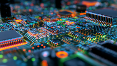
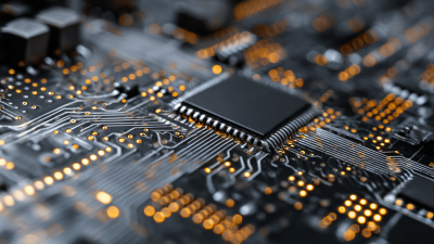
As the world of electronics continues to evolve rapidly, the demand for cutting-edge solutions in PCB circuit design is more critical than ever. The global printed circuit board (PCB) market is projected to reach $85 billion by 2025, driven by advancements in technology and the rising deployment of smart devices across various sectors. Innovations in PCB circuit design not only enhance performance but also reduce costs, thereby playing a pivotal role in promoting sustainability and efficiency in electronics manufacturing.

In light of these trends, 2025 is set to be a landmark year for PCB circuit innovations. Key developments such as flexible PCB, high-frequency circuit technology, and the integration of 5G capabilities are poised to transform the landscape of electronic devices. According to a report by Research and Markets, the flexible PCB segment alone is expected to experience a compound annual growth rate (CAGR) of 11% between 2020 and 2025, reflecting the growing need for lightweight, compact electronic systems. As we delve into the latest techniques and methodologies for designing advanced PCB circuits, it becomes evident that embracing these innovations is essential for manufacturers aiming to remain competitive in an increasingly digital world.

2025 Top PCB Circuit Innovations for Advanced Electronics and Design

Future-Ready Materials: Advancements in PCB Substrates and Their Impact

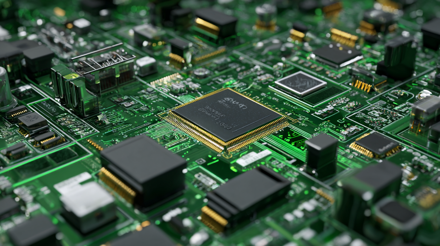
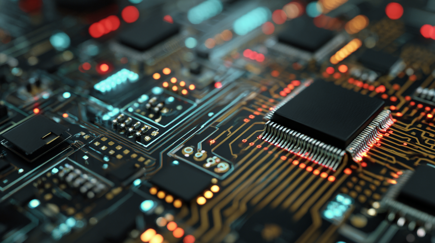
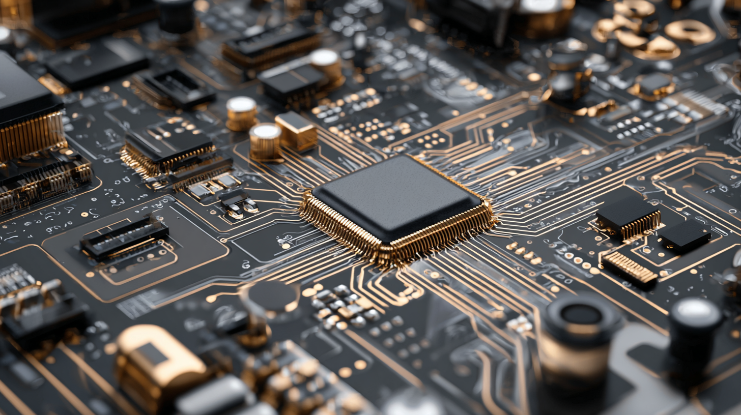
The rapid evolution of electronics has driven significant advancements in PCB (Printed Circuit Board) substrates. As technology demands higher performance, the materials used in PCB fabrication are becoming increasingly sophisticated. Future-ready materials, such as high-frequency laminates, flexible substrates, and advanced composites, are designed to support the miniaturization of components while improving signal integrity and thermal management. These innovations are crucial for applications in telecommunications, automotive systems, and robotics, where reliability and efficiency are paramount.

**Tip:** When selecting PCB substrates, consider the specific requirements of your application, such as dielectric constant, thermal conductivity, and mechanical strength. Each application may benefit from a tailored approach to materials selection to optimize performance.

As the industry progresses towards greater functionality in smaller form factors, the impact of these advanced materials becomes more evident. Enhanced substrate technologies enable better heat dissipation and reduced weight, which can lead to longer-lasting devices and improved performance in critical environments. Embracing these innovations is essential for engineers and designers who aim to stay ahead in a competitive market.

**Tip:** Stay updated with industry trends and material capabilities to make informed decisions about PCB design. Engaging with material suppliers can provide insights into the latest developments that could benefit your projects.

2025 Top PCB Circuit Innovations for Advanced Electronics and Design

High-Frequency PCB Design: Innovations for 5G and Beyond

The advancement of high-frequency PCB design is crucial as the world moves towards 5G and beyond, with industry reports predicting that the global 5G PCB market will reach $1.2 billion by 2025, reflecting a compound annual growth rate (CAGR) of 28.6% from 2020. This explosive growth underscores the necessity for innovative design practices that can support the unique demands of high-frequency applications. As operational frequencies increase, so too do the challenges associated with signal integrity, dielectric losses, and thermal management. Innovations in material science, such as low-loss dielectric substrates and advanced thermal vias, play a vital role in overcoming these challenges, allowing circuit designers to create more efficient and reliable PCBs.

Moreover, the integration of simulation-driven design tools is transforming the PCB landscape for high-frequency applications. According to a report by Research and Markets, the adoption of simulation tools in PCB design can reduce development times by up to 30%, while simultaneously improving performance metrics. These tools facilitate the exploration of complex electromagnetic behaviors and enable designers to optimize layouts for minimal crosstalk and signal degradation, which are critical in high-speed data transmission environments. As the industry continues to innovate, the convergence of advanced materials, design techniques, and simulation technologies will pave the way for the next generation of electronic devices capable of harnessing the true potential of 5G and future wireless communications.

2025 Top PCB Circuit Innovations for Advanced Electronics and Design

High-Frequency PCB Design: Innovations for 5G and Beyond

Sustainable PCB Fabrication Techniques: Greener Solutions for Electronics

The landscape of printed circuit board (PCB) fabrication is undergoing a significant transformation as sustainability becomes a pivotal focus in the electronics industry. According to a report by IPC, the trade association for the electronics industry, 70% of manufacturers are actively seeking greener practices in their production processes. This shift is driven by rising regulatory pressures and increasing consumer demand for environmentally responsible products. Innovations such as bio-based materials and advanced recycling methods are paving the way for sustainable PCB solutions, reducing the environmental footprint of electronic devices.

One prominent sustainable technique gaining traction is the use of lead-free and halogen-free materials, which significantly minimize toxicity and environmental impact. A study by the Green Electronics Council reveals that adopting such materials can reduce harmful emissions by over 30%. Furthermore, companies are investing in life cycle analysis (LCA) methodologies to assess the environmental impact of PCBs from design to disposal. As these practices become standardized, the industry can expect not only a reduction in waste but also an economic advantage, as sustainable practices often lead to reduced operational costs. With these greener solutions, the future of PCB fabrication looks promising, aligning technological advancement with ecological responsibility.

2025 Top PCB Circuit Innovations for Advanced Electronics and Design

Smart PCBs: Integrating IoT Technology for Enhanced Functionality

The integration of IoT technology into printed circuit boards (PCBs) is revolutionizing the landscape of advanced electronics. According to the 2022 PCB Manufacturing & Design Trends Report, the demand for smart PCBs is projected to grow at a CAGR of 12% over the next five years. This staggering growth is driven by the increasing need for connectivity and real-time data processing in various applications, from consumer electronics to industrial automation.

Smart PCBs equipped with IoT capabilities enhance functionality by enabling seamless communication between devices. For instance, advanced sensor integration allows for real-time monitoring and control, significantly improving operational efficiency. A recent study by IoT Analytics indicates that the global number of connected IoT devices is expected to reach 30 billion by 2025, creating vast opportunities for PCB manufacturers to innovate.

As the electronics industry continues to evolve, incorporating AI and machine learning into PCB design will further amplify the capabilities of these smart devices, ensuring they meet the demands of an increasingly interconnected world.

Flexible PCB Solutions: Redefining Design for Wearable and Mobile Devices

The landscape of electronic design is rapidly evolving, driven by the demand for more versatile and compact devices. Flexible PCB solutions are at the forefront of this transformation, particularly for wearable and mobile devices. According to a report by Market Research Future, the global flexible PCB market is projected to reach $35 billion by 2025, growing at a robust CAGR of 10.5%. This growth is primarily fueled by the increasing integration of flexible circuits in consumer electronics, medical devices, and IoT applications.

One of the standout advantages of flexible PCBs is their ability to conform to unconventional shapes, allowing for innovative product designs that were previously unattainable. For example, the adoption of flexible circuits in fitness trackers and smartwatches has revolutionized how users interact with technology, providing seamless integration into everyday wearables. Additionally, as mobile devices trend toward sleeker profiles, the lightweight and space-saving characteristics of flexible PCBs make them an ideal solution for manufacturers aiming to enhance portability without sacrificing functionality. This shift not only improves user experience but also propels advancements in battery technology and miniaturization of electronic components, further enhancing performance and efficiency in consumer electronics.

2025 Top PCB Circuit Innovations for Advanced Electronics and Design

Innovation Type Description Applications Material Used Benefits
Flexible PCB Thin, lightweight circuit boards that can bend and conform to various shapes. Wearable technology, mobile devices, medical devices. Polyimide, PET, or other flexible substrates. Space-saving, light-weight, improved performance.
Rigid-Flex PCB Combination of rigid and flexible circuits on a single board. Consumer electronics, aerospace, military applications. Copper, FR-4, flexible polyimide. Enhanced durability, reduced weight, and simplified assembly.
High-Frequency PCB Designed to effectively handle high-frequency signals. Telecommunications, radar systems, satellite communication. Rogers, Teflon, high-frequency laminates. Reduced signal loss, better signal integrity.
Multilayer PCB PCBs with three or more layers, enhancing circuit complexity. Computers, advanced medical devices, automotive electronics. FR-4, metal core, ceramic substrates. Increased circuit density, reduced interference.
3D PCB PCBs that utilize a three-dimensional structure to save space. Smartphones, laptops, IoT devices. Standard materials with added 3D construction techniques. Compact design, advanced connectivity.

Search our website