Top 10 PCB Process Techniques for Efficient Circuit Board Manufacturing?

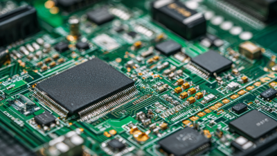
The manufacturing of printed circuit boards (PCBs) is critical in today's electronics industry. Efficient PCB process techniques can significantly impact production quality and costs. According to a recent industry report by IPC, the global PCB market reached $68.1 billion in 2022 and is expected to grow steadily. Improved processes are essential for keeping up with this rapid expansion.

Expert Dr. Emily Foster, a leader in PCB technologies, once noted, "Optimizing the PCB process is the key to achieving competitive advantage." Her insight underscores the importance of adopting advanced techniques. Despite innovations, many manufacturers still rely on outdated methods. This can lead to inefficiencies and increased costs. Additionally, the complexity of modern devices demands continual adaptation of production processes.

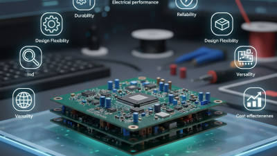
Manufacturers must evaluate their current PCB processes critically. Areas such as automation and integration of smart technologies are often overlooked. Efficiency is vital, but it should not sacrifice quality. Adopting state-of-the-art techniques like HDI and advanced soldering can enhance outcomes. Yet, it's essential to reflect on existing practices, as inefficiencies often linger unnoticed. The journey towards effective PCB process refinement is an ongoing challenge.

Top 10 PCB Process Techniques for Efficient Circuit Board Manufacturing?

Understanding the Importance of PCB Process Techniques in Manufacturing

Top 10 PCB Process Techniques for Efficient Circuit Board Manufacturing?

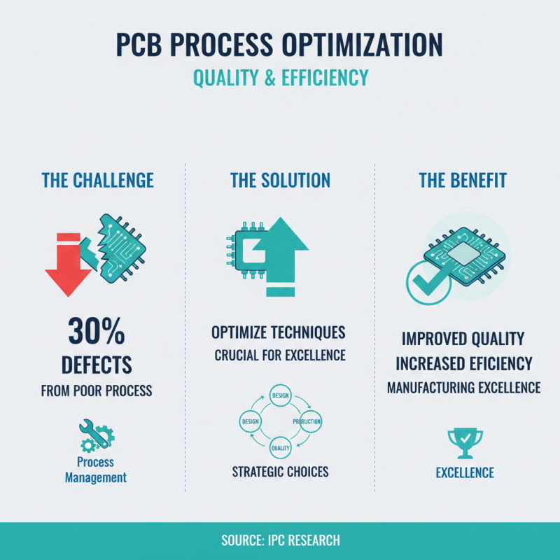
In the world of circuit board manufacturing, the techniques employed can dramatically influence both quality and efficiency. Research from IPC shows that nearly 30% of manufacturing defects stem from poor process management. Understanding and optimizing PCB process techniques is crucial for manufacturers aiming for excellence. This is not just about technology but also about strategic choices in design and production.

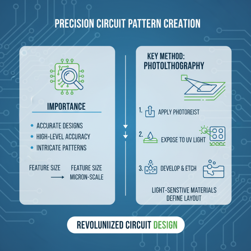
Effective techniques include precise drilling, reliable plating, and accurate imaging. For instance, data from 2022 indicates that advanced imaging technologies can reduce errors by up to 25%. However, many manufacturers still rely on outdated methods. This reliance can lead to inconsistencies and increased production costs. While automation is becoming more common, there remains a gap in staff training. Without proper training, companies risk undermining their technological investments.

Moreover, the importance of quality control cannot be overstated. Regular audits and process assessments can uncover hidden issues. By focusing on continuous improvement, manufacturers can avoid costly recalls and delays. Yet, some companies overlook this step, leading to repeated mistakes. In an industry where precision matters, neglecting PCB process techniques is a risk that many cannot afford.

Key Techniques in PCB Design for Enhanced Efficiency

When designing printed circuit boards (PCBs), efficiency is crucial. One key technique is to simplify layout designs. A clean structure minimizes signal interference and speeds up the manufacturing process. Reducing the number of layers can also save costs and time. However, this might also limit flexibility in complex designs.

Another essential technique is modular design. By breaking down the circuit into sections, each module can be designed and tested separately. This allows for easier troubleshooting and adjustments. Yet, if not managed well, integration issues may arise. It’s vital to maintain consistency across modules to avoid complexities.

Incorporating design for manufacturability (DFM) principles can enhance efficiency. These principles guide designers in creating boards that are easier to produce. It often requires adjusting design elements to align with manufacturing capabilities. It might seem tedious, but the benefits in time and cost savings are substantial. The challenge lies in balancing innovation with practicality.

Advanced Etching Methods for Precise Circuit Patterns

Top 10 PCB Process Techniques for Efficient Circuit Board Manufacturing?

Advanced etching methods are crucial for achieving precise circuit patterns in PCB manufacturing. These techniques allow manufacturers to create intricate designs with high levels of accuracy. One common method is photolithography, where light-sensitive materials help define the circuit layout. This process can create patterns as small as a few microns. It's fascinating how this technique revolutionized circuit design.

Another method is laser etching. This technique uses focused laser beams to remove material selectively. It offers flexibility in design while maintaining high precision. However, it can be costlier and requires skilled operators. Sometimes, the laser can overheat, causing unintended damage, potentially leading to rework. Manufacturers need to balance the benefits with these possible pitfalls.

Additionally, chemical etching utilizes a series of chemical baths to remove unwanted copper from the board. This method is known for its efficiency but can result in uneven patterns if not carefully controlled. The process demands close monitoring to prevent defects. Understanding these advanced methods fosters better circuit board development, yet there remains room for improvement in technique and execution.

Soldering Innovations for Reliable Electrical Connections

Soldering is a critical process in PCB manufacturing. Innovative soldering techniques enhance the reliability of electrical connections. High-quality solder joints ensure optimal performance and long-term durability. A recent industry study indicates that around 30% of PCB failures result from poor soldering techniques. Thus, manufacturers must prioritize effective soldering methods.

One effective technique is using selective soldering. This process offers precision and reduces thermal stress on sensitive components. Additionally, wave soldering remains popular for its efficiency in mass production. However, it requires careful setup to avoid defects like solder bridging.

Tips: Always perform routine checks on soldering equipment. Regular maintenance can prevent costly errors. Furthermore, training operators on the latest soldering techniques is essential. Continuous education leads to improved quality in soldering results. Remember that soldering mistakes can lead to significant production delays and loss. Reflect on the current practices and seek areas for improvement.

Quality Control Measures in PCB Production to Ensure Excellence

Quality control in PCB production is essential for achieving excellence. Manufacturers need to implement strict measures to ensure their products meet the highest standards. One common method is visual inspection. This process helps identify defects early. Inspectors check for irregularities in trace layouts, soldering quality, and component placements.

Another useful technique is Automated Optical Inspection (AOI). AOI can quickly scan boards for defects that visual inspection might miss. However, it is not foolproof. Sometimes, solder issues are hard to detect. It’s essential to back up automated methods with regular manual checks.

Tips for effective quality control:

1. Conduct regular training sessions for inspectors.
2. Utilize feedback from the production team for process improvements.
3. Develop a checklist tailored to your specific PCB processes.

Documentation can also aid quality control. Keep detailed records of inspections and tests. It helps track issues and identify patterns over time. Despite all efforts, there will be challenges. PCB manufacturing is complex. Consistently striving for improvement is vital for success.

Top 10 PCB Process Techniques for Efficient Circuit Board Manufacturing

Technique Description Benefits
Surface Mount Technology (SMT) A method where electronic components are mounted directly onto the surface of PCBs. Increased efficiency and reduced size of the circuit.
Through-Hole Technology Components are inserted into holes drilled into the PCB. Stronger mechanical connections and reliability in harsh conditions.
Electrical Testing Testing circuits for electrical continuity and functionality. Ensures quality and reduces defects.
Optical Inspection Using cameras and vision systems to inspect boards. Detects surface defects like solder issues or component misplacement.
X-Ray Inspection Using X-rays to inspect internal solder joints and components. Allows for non-destructive failures analysis.
Reflow Soldering Heating solder paste to create solder joints. Improves efficiency and ensures strong connections.
Wave Soldering Submerging PCB in molten solder to attach components. Effective for large production runs.
PCB Design for Manufacturability (DFM) Designing PCBs to optimize the manufacturing process. Reduces costs and production time.
Cleanliness and Contamination Control Ensuring PCBs are free from contaminants. Prevents failures and extends lifespan.
Thermal Management Strategies implemented to dissipate heat effectively. Enhances reliability and performance of electronic devices.

Search our website