Understanding PCB Process: A Comprehensive Guide to Modern Circuit Board Manufacturing
The modern PCB process plays a critical role in the rapidly evolving electronics industry, which is projected to reach a market value of over $60 billion by 2025. As technology advances, the demand for high-quality, efficient, and reliable circuit boards has surged, driving innovation in manufacturing techniques and materials. According to a report by IPC, the global PCB market is expanding at a compound annual growth rate (CAGR) of 5.6%, highlighting the importance of understanding the intricacies of PCB manufacturing.
This comprehensive guide delves into the various stages of the PCB process, including design, fabrication, assembly, and testing, equipping industry professionals with the knowledge necessary to navigate the complexities of modern circuit board production. By examining the latest advancements and best practices in the field, stakeholders can ensure their products meet strict industry standards while maximizing performance and cost-effectiveness.
Key Stages in PCB Manufacturing: From Design to Production
The manufacturing of printed circuit boards (PCBs) involves several critical stages, each contributing to the final product's quality and functionality.
The process begins with the design stage, where engineers use computer-aided design (CAD) software to create detailed schematics and layouts.
This initial phase is crucial, as it determines the overall configuration of the circuit board, including component placements and the routing of electrical pathways.
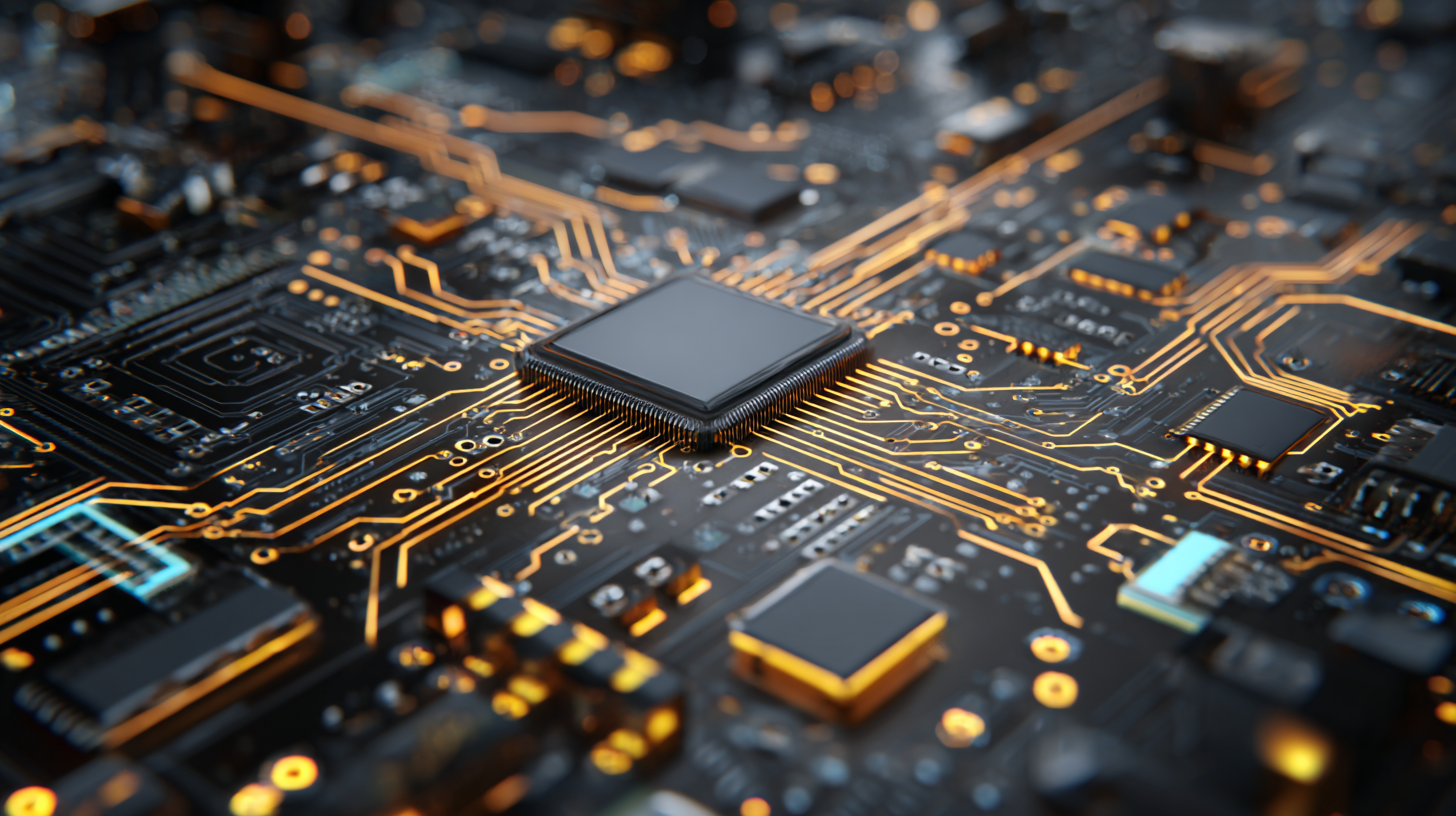
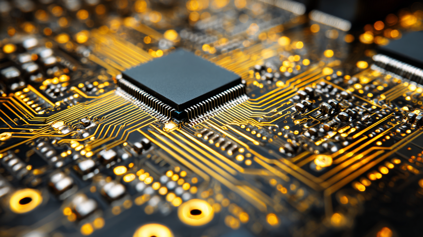
Once the design is finalized, the next stage is the fabrication of the PCB. This includes the creation of the board from materials like fiberglass and epoxy.
Techniques such as etching are employed to form the conductive pathways on the board, while drilling machines create holes for component insertion.
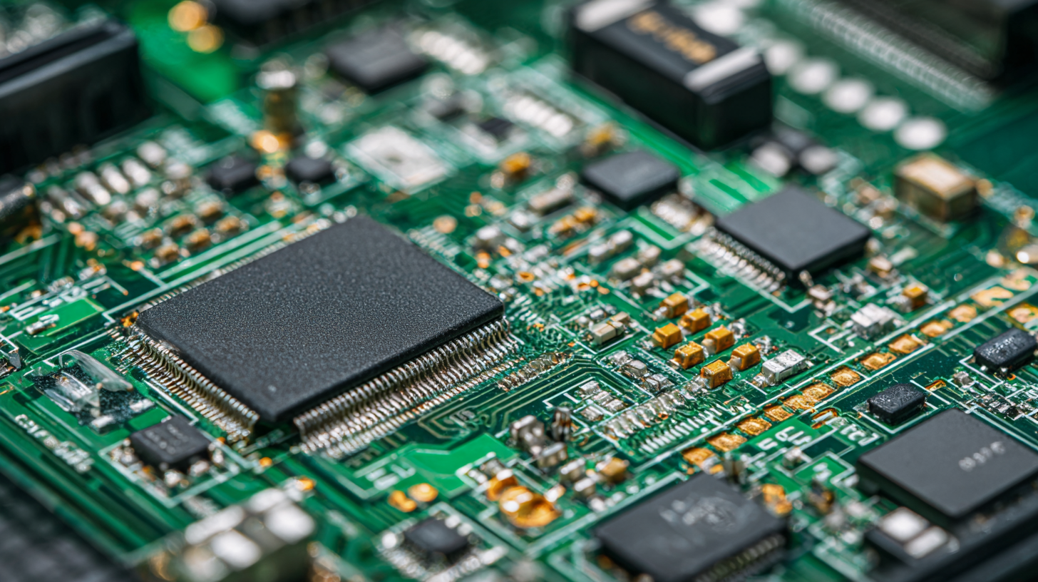
After fabrication, the PCB moves to assembly, where electronic components are soldered onto the board. This stage may involve surface mount technology (SMT) or through-hole technology,
depending on the design specifications. The process culminates with testing and inspection, ensuring that the board meets all functionality and quality standards before it is ready for deployment in various electronic devices.
Essential Materials Used in Modern Circuit Boards
In modern circuit board manufacturing, the choice of materials is crucial for ensuring optimal performance and durability. Among the primary materials used are substrates, which form the foundation of the PCB. Common substrates include fiberglass-reinforced epoxy (FR-4), which offers excellent electrical insulation and mechanical strength. This material is favored due to its lightweight nature and resistance to moisture, making it suitable for a variety of applications, from consumer electronics to industrial machinery.
Additionally, conductive materials such as copper are fundamental in facilitating electrical connections. Copper traces are etched on the PCB to form pathways for electrical signals. The thickness and quality of copper used can significantly impact the board's performance, especially in high-frequency applications. Another essential material is solder, which is used for attaching components to the PCB. Modern solders often incorporate lead-free alternatives, aligning with environmental standards while maintaining reliability. Together, these materials combine to create efficient and resilient circuit boards that meet the demands of contemporary technology.
Understanding PCB Process: A Comprehensive Guide to Modern Circuit Board Manufacturing - Essential Materials Used in Modern Circuit Boards
| Material |
Type |
Usage |
Properties |
| FR-4 |
Substrate |
Commonly used for general PCBs |
Good mechanical strength, flame retardant |
| CEM-1 |
Substrate |
Used for low-cost single-sided boards |
Basic mechanical properties, low cost |
| Copper Clad |
Conductive Layer |
Forms the electrical connections |
Excellent conductivity |
| Soldermask |
Protective Layer |
Protects against oxidation and solder bridges |
Insulation, chemical resistance |
| Silkscreen |
Marking Layer |
Used for labels and identifiers |
High contrast, visibility |
Advanced Techniques in PCB Fabrication: Innovations and Trends
The landscape of PCB fabrication is continuously evolving, driven by advancements in technology and the increasing demands of modern electronics. One of the most significant trends in the electronics manufacturing industry is the rise of advanced semiconductor packaging. These innovations are pivotal in enhancing high-performance computing (HPC) capabilities, enabling systems to operate more efficiently while meeting the escalating bandwidth requirements associated with data-intensive applications.
Additionally, there has been a surge in the emergence of startups focused on innovative PCB solutions. Out of over 1200 identified in the field, 20 standout companies are pushing the boundaries of what is possible in circuit board design and manufacturing. These startups are exploring novel materials, automation techniques, and sustainable practices, all aimed at improving production speed, reducing costs, and minimizing environmental impact. Industries are closely monitoring these trends as they play a crucial role in shaping the future of electronic devices and components.
Quality Control Measures in PCB Production for Reliability
In modern PCB manufacturing, stringent quality control measures are paramount to ensuring the reliability and performance of circuit boards. According to the IPC-A-600 standard, a critical guideline in the industry, more than 90% of defects can be prevented through effective quality assurance practices during production. This underscores the importance of implementing thorough inspection techniques throughout the PCB manufacturing process, including automated optical inspection (AOI) and X-ray inspection for hidden layers.
Tips: Regular training sessions for quality control personnel can significantly enhance defect detection skills, ensuring that teams are equipped to identify and address issues promptly.
Another vital component of quality control is the use of statistical process control (SPC), which enables manufacturers to monitor production processes in real time. According to a report published by the IPC (Institute of Printed Circuits), companies that employed SPC techniques saw a 30% reduction in defects. By analyzing statistical data, manufacturers can make informed decisions and adjustments, fostering an environment of continuous improvement.
Tips: Implementing a regular review of SPC data in production meetings can encourage proactive problem-solving and enhance team collaboration.
Quality Control Measures in PCB Production
This chart illustrates the distribution of various quality control measures implemented in modern PCB manufacturing, showcasing their significance in ensuring reliability.
Sustainability in PCB Manufacturing: Eco-friendly Practices and Their Impact
Sustainability in PCB manufacturing is increasingly gaining attention as the industry strives to reduce its environmental footprint. Recent developments highlight the importance of adopting eco-friendly practices and materials that can significantly lower the impact of production processes. For instance, a life cycle assessment approach can optimize the sustainability of printed sensors used in healthcare and environmental monitoring. By evaluating the entire lifecycle, manufacturers can identify key areas for improvement, ensuring that eco-friendly innovations, such as biodegradable substrates and solvent-free inks, are integrated into production lines.
Furthermore, the shift towards sustainable practices is exemplified by ongoing initiatives emphasizing regulatory compliance entwined with genuine environmental responsibility. Recent reports indicate that the market for sustainable electronics is projected to grow exponentially from 2025 to 2035, driven by consumer demand for greener products. The implementation of advanced technologies like metal inkjet printing is revealing how these innovations can revolutionize manufacturing processes, allowing for reduced material waste and energy consumption. Through these concerted efforts within the PCB industry, stakeholders are not only aiming for compliance but also promoting a sustainable legacy that benefits both the environment and society at large.